
Publications
(* corresponding author)
-
Hryhorii P. Parkhomenko, Andrii I. Mostovyi, Nora Schopp, Mykhailo M. Solovan, and Viktor V. Brus*, Highly Transparent Ternary Bulk-Heterojunctions for Semi-transparent Organic Photovoltaics, Journal of Materials Chemistry A (2024)

Abstract
This report presents organic ternary bulk-heterojunctions (BHJ) active layers with record average visible transmittance (AVT). The incorporation of wide bandgap organic semiconductor PTAA as a third compound into the donor diluted PCE10:COTIC-4F blend system increases AVT up to 81% and simultaneously enhances charge transport and photogeneration in the ultraviolet spectral range. Successive replacing COTIC-4F acceptor with SiOTIC-4F enhances the open-circuit voltage and elevates the opaque device performance from 4.41% to 5.77%, while maintaining the excellent AVT of the BHJ layer at around 80%. A comprehensive device physics analysis of the organic solar cells with optimized and reproducible opaque back electrode was conducted for understanding the generation– recombination processes in different donor : acceptor blends. Ultimately, semi-transparent OSCs (STOSCs) were fabricated utilizing the studied highly transparent ternary BHJ active layers demonstrating their potential for the development of semi-transparent photovoltaics.
-
Gulnur Akhtanova, Hryhorii P. Parkhomenko, Joachim Vollbrecht, Andrii I. Mostovyi, Nora Schopp, Viktor Brus*, Surface recombination in organic solar cells: Intrinsic vs. doped active layer,
Organic Electronics (2024)

Abstract
This study extends the analytical model of surface recombination in organic solar cells with an intrinsic active bulk-heterojunction layer. The key finding of the developed multi-mechanism recombination model accounting for the intrinsic active layer is that the slope of VOC vs. ln(Light Intensity) cannot be lower than 1.0 kT/q even at the extremely high concentrations of surface traps. We revealed the difference in recombination-related parameters determined in the scope of the multi-mechanism recombination model for the doped or intrinsic active layer and highlighted the importance of identifying the doping level of the active layer material. This is demonstrated by a synergy of comprehensive simulation and experimental analysis of organic solar cells with donor: acceptor blends: (PM6:Y6, PTB7-Th:COTIC-4F, PTB7-Th:O-IDTBR and PTB7-Th:ITIC-4F).
-
Hryhorii P. Parkhomenko, Mykhailo M. Solovan, Sanjay Sahare, Andriy I. Mostovyi, Damir Aidarkhanov, Nora Schopp, Taras Kovaliuk, Marat Kaikanov, Annie Ng and Viktor V. Brus*, Impact of a Short-Pulse High-Intense Proton Irradiation on High-Performance Perovskite Solar Cells, Advanced Functional Materials (2024)

Abstract
This work investigates the radiation resistance of high-performance multi-component perovskite solar cells (PSCs) for the first time under extreme short-pulse proton irradiation conditions. The devices are subjected to high-intensity 170 keV pulsed (150 ns) proton irradiation, with a fluence of up to 1013 p cm−2, corresponding to ≈30 years of operation at low Earth orbit. A complex material characterization of the perovskite active layer and device physics analysis of the PSCs before and after short-pulse proton irradiation is conducted. The obtained results indicate that the photovoltaic performance of the solar cells experiences a slight deterioration up to 20 % and 50 % following the low 2 × 10¹² p cm−2 and high 1 × 10¹³ p cm−2 proton fluences, respectively, due to increased non-radiative recombination losses. The findings reveal that multi-component PSCs are immune even to extreme high-intense short-pulse proton irradiation, which exceeds harsh space conditions, including intense coronal ejection events usually associated with solar flares.
-
Hryhorii P. Parkhomenko, Andriy I. Mostovyi, Marat Kaikanov, Jessica Strey, Mircea C. Turcu, Marvin Diederich, Sascha J. Wolter, Verena Steckenreiter, Joachim Vollbrecht* & Viktor V. Brus*, Characterization of fully-evaporated perovskite solar cells and photodetectors under high-intensity pulsed proton irradiation, Scientific Reports (2024)
_tif.png)
Abstract
This study investigates the impact of proton irradiation on perovskite devices fabricated fully through vacuum deposition. Exposure to irradiation induces changes in both electrical and optical properties. The analysis reveals that the main factors influencing the observed performance changes in solar cells are a significant reduction in shunt resistance and a minor increase in series resistance, with minimal alterations in recombination dynamics. Remarkably, the devices maintain promising photodetector characteristics both before and after proton irradiation, particularly in a self-powered mode without a reverse bias. These findings provide valuable insights into the resilience of vacuum-deposited perovskite devices against ionizing radiation, highlighting their potential for applications in radiation-prone environments, such as the nuclear industry or space exploration.
-
Nurzhan Asanov, Nora Schopp, Constantinos Valagiannopoulos, and Viktor Brus*, Optical and photovoltaic properties of organic solar cells versus bulk-heterojunction morphology,
Physical Review B (2024)
Abstract
It has long been argued that the performance of organic bulk-heterojunction solar cells critically depends on the morphology of the active layer, a mixture of donor and acceptor materials in which the charge generation from sunlight occurs. In this work, optical homogenization principles are utilized to model the structure of the common active layer PM6:Y6. By systematically modifying the size and shape of Y6 acceptor inclusions within the morphology, we explore how these changes influence the refractive index and extinction coefficient of the resulting effective medium. A synergy of transfer matrix optical simulations with the Hecht equation is used to evaluate the effect of the inclusions features on the external quantum efficiency spectrum. The reported findings can be particularly helpful in the fabrication of similar classes of organic solar cells by indicating which aspects of active layer mixture may undermine the expected performance of the photovoltaic cells.
-
Hryhorii P. Parkhomenko, Yerassyl Yerlanuly, Viktor V. Brus*, Askhat N. Jumabekov*, Effect of mild mechanical stresses on device physics of slot-die coated flexible perovskite solar cells,
Organic Electronics (2024)

Abstract
Halide perovskites are a promising class of novel photoactive materials for their application in flexible photovoltaic devices. Tolerance and stability of devices to various mechanical stresses are important aspects of this technology for its effective and long-term operation. Currently, this aspect has not been fully researched and addressed by the research community. Hence, this work is aimed at studying the effect of mild mechanical stresses (MMSs) induced by convex bending on the behaviour of ITO/ZnO/MAPbI3/Spiro-OMeTAD/Au slot-die-coated flexible perovskite solar cells (FPSCs) and investigating the underlying mechanisms leading to performance degradation in devices. The carrier generation, recombination, and extraction processes within FPSCs are investigated before and after the application of MMSs. The obtained results suggest that the photovoltaic performance of the FPSCs deteriorates by up to 50% after convex bending, due to increased non-radiative recombination losses. The results obtained in this work provide some valuable insights into the dynamics of recombination processes in FPSCs exposed to MMSs and can be used for developing new strategies for improving the mechanical stability of devices.
-
Gulnur Akhtanova, Yerassyl Yerlanuly, Hryhorii P. Parkhomenko, Mykhailo V. Solovan, Andrii I. Mostovyi, Aliya K. Nurmukhanbetova, Alexander V. Kireyev, Igor V. Danko, Pavel A. Oreshkin, Timur K. Zholdybayev, Daniyar M. Janseitov, Tlekkabul S. Ramazanov, and Viktor V. Brus*, Electron Irradiation-Induced Degradation of TiN Thin Films on Quartz and Sapphire Substrates,
ACS Omega (2024)

Abstract
In this contribution, we investigated the properties of magnetron-sputtered TiN thin films on sapphire and quartz substrates before and after 5 MeV electron irradiation with a fluence of 7 × 10¹³ e/cm2. Structural, morphological, optical, and electrical properties were analyzed to observe the impact of electron irradiation on the TiN thin films. The results showed improved electrical properties of the TiN thin films due to high-energy electron irradiation, resulting in increased specific conductivity compared to the as-deposited thin films on both sapphire and quartz substrates. The structural features of the TiN thin films on the sapphire substrate transformed from polycrystalline to amorphous, while the TiN thin films deposited on the quartz substrate remained unchanged. Chemical state analysis indicated changes in the metallic bonding between Ti and N in the deposited TiN on the sapphire substrate, while TiN deposited on the quartz substrate retained its Ti–N bonding. This study provides insights into the effects of electron irradiation on TiN thin films, emphasizing the importance of investigating radiation resistance for the reliable operation of optoelectronic devices and photovoltaic systems in extreme ionizing radiation environments.
-
Zhifang Du, Hoang Mai Luong, Sina Sabury, Austin L. Jones, Ziyue Zhu, Patchareeporn Panoy, Sangmin Chae, Ahra Yi, Hyo Jung Kim, Steven Xiao, Viktor V. Brus, G. N. Manjunatha Reddy, John R. Reynolds, Thuc-Quyen Nguyen, High-Performance Wearable Organic Photodetectors by Molecular Design and Green Solvent Processing for Pulse Oximetry and Photoplethysmography,
Advanced Materials (2024)

Abstract
White-light detection from the visible to the near-infrared region is central to many applications such as high-speed cameras, autonomous vehicles, and wearable electronics. While organic photodetectors (OPDs) are being developed for such applications, several challenges must be overcome to produce scalable high-detectivity OPDs. This includes issues associated with low responsivity, narrow absorption range, and environmentally friendly device fabrication. Here, an OPD system processed from 2-methyltetrahydrofuran (2-MeTHF) sets a record in light detectivity, which is also comparable with commercially available silicon-based photodiodes is reported. The newly designed OPD is employed in wearable devices to monitor heart rate and blood oxygen saturation using a flexible OPD-based finger pulse oximeter. In achieving this, a framework for a detailed understanding of the structure–processing–property relationship in these OPDs is also developed. The bulk heterojunction (BHJ) thin films processed from 2-MeTHF are characterized at different length scales with advanced techniques. The BHJ morphology exhibits optimal intermixing and phase separation of donor and acceptor moieties, which facilitates the charge generation and collection process. Benefitting from high charge carrier mobilities and a low shunt leakage current, the newly developed OPD exhibits a specific detectivity of above 1012 Jones over 400–900 nm, which is higher than those of reference devices processed from chlorobenzene and ortho-xylene.
-
Weiquan Chen, Yuhui Qiu, Ivan S. Babichuk, Yu Chang, Ruiliang Zhou, Zifeng He, Yijie Liu, Jianan Zhang, Iryna V. Babichuk, Anton Tiutiunnyk, David Laroze, Viktor V. Brus, Jian Yang, Improving the Strain Control Performance of MoS2 Monolayer to Develop Flexible Electronics,
Advanced Engineering Materials (2024)

Abstract
In recent years, two-dimensional (2D) materials with unique mechanical, optical, and electrical properties have attracted extensive attention. In terms of mechanical properties, 2D molybdenum disulfide (MoS2) can perform larger strains than traditional semiconductor materials. In this contribution, the chemical vapor deposition technique to grow MoS2 films on a Si wafer and transfer them onto a flexible substrate is used. The controlled deformation of 2D MoS2 samples is realized by encapsulating them with a flexible acrylate film via successive spin-coating and photopolymerization. Improved strain control is achieved due to the perfect integration of different components (MoS2/substrate) and the high adhesion of polymers. This approach provides a better detection of the changing structure of the MoS2 monolayer on the flexible substrate during tensile. It is noted that the crystal symmetry damage caused by strain is reflected in the redshift of the characteristic bands of MoS2. Hence, an effective way for strain regulation of MoS2 for future applications in flexible devices is provided.
-
Nora Schopp, Ernazar Abdikamalov, Andrii I. Mostovyi, Hryhorii P. Parkhomenko, Mykhailo M. Solovan, Ernest A. Asare, Guillermo C. Bazan, Thuc-Quyen Nguyen, George F. Smoot & Viktor V. Brus*, Interstellar photovoltaics, Scientific Reports (2023)

Abstract
The term 'Solar Cell’ is commonly used for Photovoltaics that convert light into electrical energy. However, light can be harvested from various sources not limited to the Sun. This work considers the possibility of harvesting photons from different star types, including our closest neighbor star Proxima Centauri. The theoretical efficiency limits of single junction photovoltaic devices are calculated for different star types at a normalized light intensity corresponding to the AM0 spectrum intensity with AM0 = 1361 W/m2. An optimal bandgap of > 12 eV for the hottest O5V star type leads to 47% Shockley-Queisser photoconversion efficiency (SQ PCE), whereas a narrower optimal bandgap of 0.7 eV leads to 23% SQ PCE for the coldest red dwarf M0, M5.5Ve, and M8V type stars. Organic Photovoltaics (OPVs) are the most lightweight solar technology and have the potential to be employed in weight-restricted space applications, including foreseeable interstellar missions. With that in mind, the Sun’s G2V spectrum and Proxima Centauri’s M5.5Ve spectrum are considered in further detail in combination with two extreme bandgap OPV systems: one narrow bandgap system (PM2:COTIC-4F, Eg = 1.14 eV) and one wide bandgap system (PM6:o-IDTBR, Eg = 1.62 eV). Semi-empirically modeled JV-curves reveal that the absorption characteristics of the PM2:COTIC-4F blend match well with both the G2V and the M5.5Ve spectrum, yielding theoretical PCEs of 22.6% and 12.6%, respectively. In contrast, the PM6:o-IDTBR device shows a theoretical PCE of 18.2% under G2V illumination that drops sharply to 0.9% under M5.5Ve illumination.
-
Yerassyl Yerlanuly, Hryhorii P. Parkhomenko, Rakhymzhan Ye Zhumadilov, Renata R. Nemkayeva, Gulnur Akhtanova, Mykhailo M. Solovan, Andrii I. Mostovyi, Sagi A. Orazbayev, Almasbek U. Utegenov, Tlekkabul S. Ramazanov, Maratbek T. Gabdullin, Askhat N. Jumabekov, Viktor V. Brus*, Achieving stable photodiode characteristics under ionizing radiation with a self-adaptive nanostructured heterojunction CNWs/CdZnTe, Carbon (2023)

Abstract
This study proposed self-adaptive nanostructured heterojunction UV-VIS-NIR photodiodes carbon nanowalls (CNWs)/cadmium zinc telluride (CdZnTe) exhibiting stable photoelectric characteristics under ionizing radiation conditions. We carried out a comprehensive analysis of the impact of proton radiation with an energy of 1.5 MeV and a total fluence of 1012 protons/cm2 on the properties of CNWs and CdZnTe functional layers, as well as on the main photodiode characteristics of the CNWs/CdZnTe heterojunctions, employing a set of state-of-the-art materials and device characterization techniques. Responsivity and detectivity of the prepared heterojunctions even slightly improve after exposure to harsh ionizing radiation conditions due to the unique radiation-induced self-adaptive features of the CNWs/CdZnTe heterojunction interface. The characteristics of the CNWs/CdZnTe photodiodes before and after high-energy proton bombardment demonstrate excellent stability, which is the key requirement for long-term and reliable operation of optoelectronic devices in space or radioactively contaminated environments.
-
Hryhorii P. Parkhomenko, Andriy I. Mostovyi, Gulnur Akhtanova, Mykhailo M. Solovan,
Marat Kaikanov, Nora Schopp, and Viktor V. Brus*, Self-Healing of Proton-Irradiated Organic Photodiodes and Photovoltaics, Advanced Energy Materials (2023)

Abstract
In this study, a comprehensive quantitative analysis of the photodiode (PD) is conducted and photovoltaic (PV) characteristics of organic non-fullerene PCE10:ITIC-4F devices before and after exposure to a 150 ns pulse of 170 keV proton irradiation with the fluence of 2·1012 p cm−2 that is equivalent to ≈6 years of operation at a low Earth orbit. While an expected initial performance reduction happened in the photodiode and photovoltaic operation modes, a hitherto unknown self-healing effect in the organic devices is observed several days after the proton irradiation. The organic bulk-heterojunction (BHJ) material properties and the multi-mechanisms recombination processes before and after irradiation and during self-healing are investigated. This analysis provides a quantitative understanding of the changes occurring in the device physics and points toward the relevant aspects of the self-healing mechanism related to the dynamics of proton-induced traps in the bulk of the organic active layer. Ultimately, the synergy of record lightweight features and newly discovered self-healing of proton-induced damage in organic PDs and solar cells highlights their great potential for applications in rapidly emerging space technology.
-
Nora Schopp, Sina Sabury, Thomas Chaney, Junxiang Zhang, Hiba Wakidi, Brian M. Kim, Rahul Sankar, Hoang M. Luong, Pattarawadee Therdkatanyuphong, Viktor V. Brus, Seth Marder,* Michael F. Toney,* John R. Reynolds,* and Thuc-Quyen Nguyen*, Organic Photovoltaic Performance Resiliency: Role of Molecular Weight in a PM7 Derivative, ACS Energy Lett. (2023)

Abstract
Batch-to-batch variations remain a challenge for organic photovoltaics (OPVs) that must be solved for widespread commercialization. This work addresses the role of the molecular weight (MW), introducing a new donor polymer PM7-D5 with an extended thiophene bridge compared to that of PM6 or PM7. Devices comprising PM7-D5 and the nonfullerene acceptor L8-BO are relatively insensitive to a significant molecular weight variation and result in OPVs with photoconversion efficiencies (PCEs) of 11.4% and 12.4%, when using polymers with 26 and 125 kDa. We elucidate the origins of the small performance change and systematically address morphology, charge generation, recombination, and extraction, combining optical simulations and experimental techniques. The comprehensive analysis emphasizes the complexity of the photoelectric processes and confirms the high robustness to MW variations of this blend system. Lastly, we review reported blends and suggest systematic research of the structural parameters that lead to an increased robustness to MW changes.
Mykhailo M. Solovan, Andriy I. Mostovyi, Damir Aidarkhanov, Hryhorii P. Parkhomenko,
Gulnur Akhtanova, Nora Schopp, Ernest A. Asare, Dosbol Nauruzbayev,
Marat Kaikanov, Annie Ng, and Viktor V. Brus*, Extreme Radiation Resistance of Self-Powered High-Performance Cs0.04Rb0.04(FA0.65MA0.35)0.92Pb(I0.85Br0.14Cl0.01)3 Perovskite Photodiodes, Advanced Optical Materials (2023)

Abstract
This work reports, for the first time, on radiation resistance of state-of-the-art multicomponent Cs0.04Rb0.04(FA0.65MA0.35)0.92Pb(I0.85Br0.14Cl0.01)3 perovskite photodiodes, tested under high-intensity pulsed 170 keV proton irradiation with fluence up to 1013 protons cm−2. The studied photodiodes demonstrate record radiation resistance among reported analogous optoelectronic devices. Specifically, it is shown that the proton irradiation with the fluence of 2 × 10¹² protons cm−2 even leads to a slight improvement in the photodiode parameters. Nonetheless, a large fluence of 1013 protons cm−2 deteriorates photodiode parameters on average by only 25% with respect to that of the as-prepared devices. The revealed high-performance and advanced radiation hardness demonstrate the huge application potential of lightweight and low-cost solution-processed perovskite optoelectronic devices in sensing and communication networks operating under harsh space conditions.
Andrii I Mostovyi, Serhii І Kuryshchuk, Nurzhan Asanov, Hryhorii P Parkhomenko, Taras T Kovaliuk, Ivan G Orletskyi, Mykhailo M Solovan and Viktor V Brus*, A self-powered UV–vis–NIR graphite/CdZnTe Schottky junction photodiode, Semiconductor Science and Technology (2023)

Abstract
We proposed a self-powered UV–vis–NIR Schottky junction photodiode based on a unique combination of radiation-hard functional materials: thin-film semi-metal Graphite and CdZnTe single-crystal compound semiconductor. The graphite/CdZnTe Schottky junction photodiodes exhibit a maximum responsivity of 0.25 A W−1 and detectivity of 6.5 × 10¹¹ Jones, close to the best heterojunction photodiodes based on CdZnTe solid solution. The devices are also characterized by short rise/fall times (1.2/7.2 µs) and a wide linear dynamic range (77 dB). The proposed photodiodes are promising for applications in space and terrestrial areas with high levels of ionizing radiation.
Nora Schopp, Gulnur Akhtanova, Patchareepond Panoy, Alexandr Arbuz, Sangmin Chae, Ahra Yi, Hyo Jung Kim, Vinich Promarak, Thuc-Quyen Nguyen and Viktor V. Brus*, Unraveling Device Physics of Dilute-Donor Narrow Band Gap Organic Solar Cells with Highly Transparent Active Layers, Advanced Materials (2022)

Abstract
This work investigates the charge generation-recombination dynamics in three narrow band gap near-IR absorbing NFA-based OPV systems with varied donor concentrations of 40%, 30%, and 20%. The dilution of the polymer donor with visible-range absorption leads to highly transparent active layers with blend AVTs of 64%, 70%, and 77%, respectively. Opaque devices in the optimized highly-reproducible device configuration comprising these transparent active layers lead to PCEs of 7.0%, 6.5%, and 4.1%. The investigation of these structures yields quantitative insights into changes in the charge generation, non-geminate charge recombination, and extraction dynamics upon dilution of the donor. Lastly, we give an outlook for employing the highly transparent active layers in ST-OPVs.
M. M. Solovan, A. I. Mostovyi, H. P. Parkhomenko, M. Kaikanov, N. Schopp, E. A. Asare, T. Kovaliuk, P. Veřtát, K. S. Ulyanytsky, D. V. Korbutyak, V. V. Brus*, A High‐Detectivity, Fast‐Response, and Radiation‐Resistant TiN/CdZnTe Heterojunction Photodiode,
Advanced Optical Materials (2022)

Abstract
A novel high-performance ultraviolet–visible–near-infrared (300–820 nm) heterojunction photodiode based on radiation-resistant semiconductor materials is proposed. A titanium nitride (TiN) “window” layer is deposited via magnetron sputtering onto a cadmium zinc telluride (CdZnTe) solid solution single crystal. The TiN/CdZnTe heterojunction photodiodes concurrently reveal an outstanding detectivity, response time, and linear dynamic range outperforming similar heterojunction photodiodes and photodetectors, based on photoactive inorganic compound semiconductor materials. Moreover, the added feature of the proposed heterojunction photodiodes is their excellent radiation resistance, experimentally demonstrated under short impulse proton irradiation (170 keV) with an accumulated fluence of 2 × 10¹² proton cm−2. This unusual synergy of high performance and advanced radiation resistance of the TiN/CdZnTe photodiodes provides a unique platform for operation in space or radioactively contaminated environments.

Abstract
In this work, a complex experimental study of the effect of electron and proton ionizing radiation on the properties of carbon nanowalls (CNWs) is carried out using various state-of-the-art materials characterization techniques. CNW layers on quartz substrates were exposed to 5 MeV electron and 1.8 MeV proton irradiation with accumulated fluences of 7 × 10¹³ e/cm2 and 1012 p/cm2, respectively. It is found that depending on the type of irradiation (electron or proton), the morphology and structural properties of CNWs change; in particular, the wall density decreases, and the sp2 hybridization component increases. The morphological and structural changes in turn lead to changes in the electronic, optical, and electrical characteristics of the material, in particular, change in the work function, improvement in optical transmission, an increase in the surface resistance, and a decrease in the specific conductivity of the CNW films. Lastly, this study highlights the potential of CNWs as nanostructured functional materials for novel high-performance radiation-resistant electronic and optoelectronic devices.
Nora Schopp and Viktor V. Brus*, A Review on the Materials Science and Device Physics of Semitransparent Organic Photovoltaics, Energies (2022)

Abstract
In this review, the current state of materials science and the device physics of semitransparent organic solar cells is summarized. Relevant synthetic strategies to narrow the band gap of organic semiconducting molecules are outlined, and recent developments in the polymer donor and near-infrared absorbing acceptor materials are discussed. Next, an overview of transparent electrodes is given, including oxides, multi-stacks, thin metal, and solution processed electrodes, as well as considerations that are unique to ST-OPVs. The remainder of this review focuses on the device engineering of ST-OPVs. The figures of merit and the theoretical limitations of ST-OPVs are covered, as well as strategies to improve the light utilization efficiency. Lastly, the importance of creating an in-depth understanding of the device physics of ST-OPVs is emphasized and the existing works that answer fundamental questions about the inherent changes in the optoelectronic processes in transparent devices are presented in a condensed way. This last part outlines the changes that are unique for devices with increased transparency and the resulting implications, serving as a point of reference for the systematic development of next-generation ST-OPVs.
Joachim Vollbrecht, Nurlan Tokmoldin, Bowen Sun, Viktor V. Brus, Safa Shoaee, and Dieter Neher, Determination of the charge carrier density in organic solar cells: A tutorial,
Journal of Applied Physics (2022)

Abstract
The increase in the performance of organic solar cells observed over the past few years has reinvigorated the search for a deeper understanding of the loss and extraction processes in this class of device. A detailed knowledge of the density of free charge carriers under different operating conditions and illumination intensities is a prerequisite to quantify the recombination and extraction dynamics. Differential charging techniques are a promising approach to experimentally obtain the charge carrier density under the aforementioned conditions. In particular, the combination of transient photovoltage and photocurrent as well as impedance and capacitance spectroscopy have been successfully used in past studies to determine the charge carrier density of organic solar cells. In this Tutorial, these experimental techniques will be discussed in detail, highlighting fundamental principles, practical considerations, necessary corrections, advantages, drawbacks, and ultimately their limitations. Relevant references introducing more advanced concepts will be provided as well. Therefore, the present Tutorial might act as an introduction and guideline aimed at new prospective users of these techniques as well as a point of reference for more experienced researchers.
N. Schopp, H.M. Luong, B.R. Luginbuhl, P. Panoy, D. Choi, V. Promarak, V.V. Brus*,
T.-Q. Nguyen*, Understanding Interfacial Recombination Processes in Narrow-Band-Gap Organic Solar Cells, ACS Energy Letters (2022)

Abstract
Recombination losses in organic photovoltaics (OPVs) remain a performance-limiting factor, including bulk trap-assisted recombination and interfacial recombination at the electrode:active layer interface. In this work, we demonstrate the role of the front electrode:active layer interface in a narrow-band-gap system, PCE10:COTIC-4F, a promising candidate for semitransparent organic photovoltaics. We systematically address charge generation, recombination, and extraction, with a focus on interfacial recombination via surface traps by a comparison of four device structures with electrodes based on ZnO, ZnO/PFN-Br, PEDOT:PSS, and a self-doped conjugated polyelectrolyte (CPE-K). The amount of interfacial recombination is affected significantly by the electrode choice, while similar levels of bulk recombination are maintained. For the studied blend, we identify ZnO as a suitable choice, pairing low surface recombination rates with beneficial charge carrier generation, favorable energy level alignment, and efficient extraction. In contrast, PEDOT:PSS-based devices suffer from interfacial recombination, which can be suppressed when CPE-K is used instead.
V.V. Brus*, M.M. Solovan, N. Schopp, M. Kaikanov, A.I. Mostovyi,
Visible to Near-Infrared Photodiodes with Advanced Radiation Resistance,
Advanced Theory and Simulations (2022)

Abstract
A new type of sub-micron metal-intrinsic semiconductor-metal visible to near-infrared (400–1600 nm) photodiodes based on a unique combination of radiation-resistant functional materials: sapphire, TiN, MoOx, CdTe, Hg3In2Te6, and graphite is proposed. The promising optoelectronic characteristics are calculated in the scope of a comprehensive semi-analytical model, based on the complementary fusion of numerical Transfer Matrix optical simulation with analytical Hecht and dark generation current equations. The findings demonstrate proof-of-concept next-generation high-performance optoelectronic devices with advanced radiation resistance. Moreover, a simple device engineering modification has revealed a significant optimization potential for considered photodiodes.
Y. Yerlanuly, R. Zhumadilov, R. Nemkayeva, B. Uzakbaiuly, A. R. Beisenbayev, Z. Bakenov, T. Ramazanov, Maratbek Gabdullin, Annie Ng, Viktor V. Brus* and Askhat N. Jumabekov*, Physical Properties of Carbon Nanowalls Synthesized by the ICP-PECVD Method vs. the Growth Time,
Scientific Reports 11 (2021) 19287
Abstract
Investigation of the physical properties of carbon nanowall (CNW) films is carried out in correlation with the growth time. The structural, electronic, optical and electrical properties of CNW films are investigated using electron microscopy, Raman spectroscopy, X-ray photoelectron spectroscopy, ultraviolet photoelectron spectroscopy, UV–Vis spectroscopy, Hall Effect measurement system, Four Point Probing system, and thermoelectric measurements. Shorter growth time results in thinner CNW films with a densely spaced labyrinth structure, while a longer growth time results in thicker CNW films with a petal structure. These changes in morphology further lead to changes in the structural, optical, and electrical properties of the CNW.
J. Vollbrecht* and V.V. Brus*, Effects of Recombination Order on Open-Circuit Voltage Decay Measurements of Organic and Perovskite Solar Cells, Energies 14 (2021) 4800

Abstract
Non-geminate recombination, as one of the most relevant loss mechanisms in organic and perovskite solar cells, deserves special attention in research efforts to further increase device performance. It can be subdivided into first, second, and third order processes, which can be elucidated by the effects that they have on the time-dependent open-circuit voltage decay. In this study, analytical expressions for the open-circuit voltage decay exhibiting one of the aforementioned recombination mechanisms were derived. It was possible to support the analytical models with experimental examples of three different solar cells, each of them dominated either by first (PBDBT:CETIC-4F), second (PM6:Y6), or third (irradiated CH3NH3PbI3) order recombination. Furthermore, a simple approach to estimate the dominant recombination process was also introduced and tested on these examples. Moreover, limitations of the analytical models and the measurement technique itself were discussed.
N. Schopp, T.-Q. Nguyen* and V.V. Brus*, Optical Expediency of Back Electrode Materials for Organic Near-Infrared Photodiodes, ACS Applied Mater. and Interfaces 13 (2021) 27217–27226
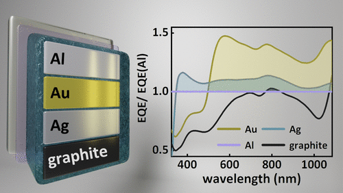
Abstract
Organic semiconductor devices, including organic photodetectors (OPDs) and organic photovoltaics (OPVs), have undergone vast improvements, thanks to the development of non-fullerene acceptors. The absorption range of such NFA-based systems is typically shifted toward the near-infrared (near-IR) region compared to early-generation fullerene-based systems, rendering organic semiconductor devices suitable for near-IR sensing applications. While most efforts are concentrated on the photoactive materials, less attention is paid to the impact of the back electrodes on the device performance. Therefore, this work focuses on the optical expediency of gold (Au), silver (Ag), aluminum (Al), and graphite as back electrode materials in organic optoelectronics. This work shows that the “one size fits all” methodology is not a valid approach for choosing the back electrode material. Instead, considering the active layer absorption, the active layer thickness, and the intended application is necessary. A traditional polymer/fullerene-based system, poly(3-hexylthiophene) with [6,6]-phenyl C61 butyric acid methyl ester (P3HT:PC60BM), and a state-of-the-art narrow-band gap non-fullerene-based system, poly[4,8bis(5-(2-ethylhexyl)thiophen-2-yl)benzo[1,2-b; 4,5-b′]dithiophene-2,6-diyl-alt-(4-(2-ethy-lhexyl)3-fluorothieno[3,4-b]thiophene-)-2-carboxylate-(2-6-diyl)] and 2,2′-((2Z,2′Z)-((5,5′-(4,4-bis(2-ethylhexyl)4H-cyclopenta[1,2-b:5,4-b′]dithiophene-2,6-diyl)bis(4-((2ethylhexyl)oxy)thiophene-5,2-diyl))bis(methanylylidene)) bis(5,6-difluoro3-oxo-2,3-dihydro-1H-indene-2,1-diylidene))dimalononitrile (PCE10:COTIC-4F), are investigated by combining optical transfer matrix modeling simulations with experimentally determined recombination and extraction losses. We find that the narrow-band gap system shows performance gains when employing Au as the back electrode. Furthermore, we show that these performance gains are dependent on active layer thickness, yielding the most significance for thin active layers (<100 nm). Such thin, ultra-narrow-band gap devices are the focus of near-IR sensing applications, highlighting the importance of methodically choosing the back electrode. Lastly, the impact of the back electrode on the OPV device performance is outlined.
N. Schopp, V.V. Brus, J. Lee, A. Dixon, A. Karki, T. Liu, Z. Peng, K.R. Graham, H. Ade, G.C. Bazan,
T.-Q. Nguyen*, Effect of Palladium-tetrakis(triphenylphosphine) Catalyst Traces on Charge Recombination and Extraction in Non-Fullerene-based Organic Solar Cells,
Advanced Functional Materials 31 (2021) 2009363.

Abstract
The effect of the cross-coupling catalyst tetrakis(triphenylphosphine)palladium(0) (Pd(PPh3)4) on the performance of a model organic bulk-heterojunction solar cell composed of a blend of poly([2,6′-4,8-di(5-ethylhexylthienyl)benzo[1,2-b;3,3-b]dithiophene]{3-fluoro-2[(2-ethylhexyl)carbonyl]thieno[3,4-b]thiophenediyl}) (PTB7-Th) donor and 3,9-bis(2-methylene-((3-(1,1-dicyanomethylene)-6,7-difluoro)-indanone))-5,5,11,11-tetrakis(4-hexylphenyl)-dithieno[2,3-d:2′,3′-d′]-s-indaceno[1,2-b:5,6-b′]dithiophene (IOTIC-4F) non-fullerene acceptor is investigated. The effect of intentional addition of different amounts of Pd(PPh3)4 on morphology, free charge carrier generation, non-geminate bulk trap- and surface trap-assisted recombination as well as bimolecular recombination and charge extraction is quantified. This work shows that free charge carrier generation is affected significantly, while the impact of Pd(PPh3)4 on non-geminate recombination processes is limited because the catalyst does not facilitate efficient trap-assisted recombination. The studied system shows substantial robustness towards the addition of Pd(PPh3)4 in small amounts.
V.V. Brus*, N. Schopp, S.-J. Ko, J. Vallbrecht, J. Lee, A. Karki, G. C. Bazan, Q.-T. Nguyen*, Temperature and Light Modulated Open-Circuit Voltage in Non-Fullerene Organic Solar Cells with Different Effective Bandgaps, Advanced Energy Materials 11 (2021) 202003091

Abstract
The relationship of the temperature–light intensity dependence of open-circuit voltage Voc in nonfullerene-based organic solar cells with their material characteristics and multimechanism recombination parameters is described. The systematic variation of the effective bandgap Eg,eff and the electrode layers allows the observation of different relative contributions of bimolecular, bulk, and surface trap-assisted recombination mechanisms. The complementary advantages of the analytical model and the established voltage-impedance spectroscopy technique provide a useful tool to quantify multimechanism recombination parameters, effective density of states Nc, and energetic disorder σ in organic solar cells under operating conditions. The validity of the proposed model to understand the temperature and light intensity dependent of Voc is shown by applying it to four different donor:nonfullerene acceptor blend systems with conventional or inverted device architectures.
N. Schopp, V.V. Brus*, T.-Q. Nguyen*, On Optoelectronic Processes in Organic Solar Cells: from Opaque to Transparent, Advanced Optical Materials 9 (2021) 2001484

Abstract
Organic (semi)transparent photovoltaics (ST-OPVs) promise integrated, sustainable, low-cost energy harvesting solutions. However, current efficiency limitations have to be overcome to make ST-OPV a competitive technology. In this simulation-based work, the effect of the selective transparency on the photoelectronic processes in ST-OPVs is studied and changes in the generation–recombination dynamics and the extraction efficiency are demonstrated that are causally linked to the increased transparency. The study of five model systems with transparent indium tin oxide (ITO) back electrodes and systematically varied extinction coefficients and an opaque cell with Ag back contact allows to quantify these changes in the photoelectronic processes and to address the role of the series and the shunt resistors while keeping all other parameters of the modeled devices identical. The findings demonstrate the increased importance of the active layer quality in ST-OPVs and indicate that ST-OPVs benefit from a wider choice of transparent electrode materials.
N. Schopp, V.V. Brus*, J. Lee, G.C. Bazan, T.-Q. Nguyen*, A simple Approach for Unraveling Optoelectronic Processes in Organic Solar Cells Under Short-Circuit Conditions,
Advanced Energy Materials 11 (2021) 2002760

Abstract
The short-circuit current (Jsc) of organic solar cells is defined by the interplay of exciton photogeneration in the active layer, geminate and non-geminate recombination losses and free charge carrier extraction. The method proposed in this work allows the quantification of geminate recombination and the determination of the mobility-lifetime product (µτ) as a single integrated parameter for charge transport and non-geminate recombination. Furthermore, the extraction efficiency is quantified based on the obtained µτ product. Only readily available experimental methods (current-voltage characteristics, external quantum efficiency measurements) are employed, which are coupled with an optical transfer matrix method simulation. The required optical properties of common organic photovoltaic (OPV) materials are provided in this work. The new approach is applied to three OPV systems in inverted or conventional device structures, and the results are juxtaposed against the µτ values obtained by an independent method based on the voltage–capacitance spectroscopy technique. Furthermore, it is demonstrated that the new method can accurately predict the optimal active layer thickness.
W. Quyang, Y. Li, B. Yurash, N. Schopp, A. Vega-Flick, V.V. Brus, T.-Q. Nguyen, B. Liao*, Transient Gating Spectroscopy of Photocarrier Dynamics in Semiconducting Polymer Thin Films,
Applied Physics Letters, 117 (2020) 253302
Abstract
While charge carrier dynamics and thermal management are both keys to the operational efficiency and stability for energy-related devices, experimental techniques that can simultaneously characterize both properties are still lacking. In this paper, we use laser-induced transient grating (TG) spectroscopy to characterize thin films of the archetypal organic semiconductor regioregular poly(3-hexylthiophene) and its blends with the electron acceptor [6,6]-phenyl-C61-butyric acid methyl ester on glass substrates. While the thermal responses from the thin film and the substrate cannot be distinguished due to their similar thermal diffusivities, we show that the recombination dynamics of photocarriers in the organic semiconductor thin films occur on a similar timescale and can be separated from the thermal response. Our measurements indicate that the photocarrier dynamics are determined by multiple recombination processes and our extracted recombination rates are in good agreement with previous reports using other techniques. We further apply TG spectroscopy to characterize another conjugated polymer and a molecular fluorescent material to demonstrate its general applicability. Our study indicates the potential of transient grating spectroscopy to simultaneously characterize thermal transport and photocarrier dynamics in organic optoelectronic devices.
J. Vollbrecht* and V.V. Brus*, On Charge Carrier Density in Organic Solar Cells Obtained via Capacitance Spectroscopy, Advanced Electronic Materials 6 (2020) 2000517

Abstract
The determination of the voltage-dependent density of free charge carriers via capacitance spectroscopy is considered an important step in the analysis of emerging photovoltaic technologies, such as organic and perovskite solar cells. In particular, an intimate knowledge of the density of free charge carriers is required for the determination of crucial parameters such as the effective mobility, charge carrier lifetime, nongeminate recombination coefficients, average extraction times, and competition factors. Hence, it is paramount to verify the validity of the commonly employed approaches to obtain the density of free charge carriers. The advantages, drawbacks, and limitations of the most common approaches are investigated in detail and strategies to mitigate misleading values are explored. To this end, two types of nonfullerene organic solar cells based on a PTB7-Th:ITIC-2F blend and a PM6:Y6 blend, respectively, are used as a case study to assess how subsequent analyses of the nongeminate recombination dynamics depend on the chosen approach to calculate the density of free charge carriers via capacitance spectroscopy.
V.V. Brus*, M.I. Ilashchuk, I.G. Orletskyi, M.M. Solovan, G.P. Parkhomenko, I.S. Babichuk, N. Schopp, G.O. Andrushchak, A.I. Mostovyi, P.D. Maryanchuk, Coupling Between Structural Properties and Charge Transport in Nano-Crystalline and Amorphous Graphitic Carbon Films, Deposited by Electron-Beam Evaporation, Nanotechnology 31 (2020) 505706
Abstract
Nano-crystalline and amorphous films of graphitized carbon were deposited by electron-beam evaporation of bulk graphite. Structural properties and the size of graphite nanoclusters (L ≈ 1.2–5 nm) in the films were determined from the analysis of their Raman spectra. Electrical properties of the bulk nano-crystalline graphite reference sample and the deposited graphitic carbon films were measured by means of the Hall effect technique within the temperature range from 290 to 420 K. The electrical conductivity σ and Hall mobility μH of all samples exhibited exponential temperature dependences, indicating on the non-metallic behavior. Electrical properties of the amorphous graphitic carbon thin films, deposited at low substrate temperatures (620 and 750 K) were analyzed in the scope of the hopping charge transport mechanism via localized states. We have shown that the charge transport in the bulk and thin film (920 K) nano-crystalline graphite samples is carried out via the tunneling and thermionic emission over potential barriers at the grain boundaries.This paper contributes towards better understanding of coupling between structural and electrical properties of graphitic carbon thin films.
J. Vollbrecht* and V.V. Brus*, On the Recombination Order of Surface Recombination under Open Circuit Conditions, Organic Electronics 86 (2020) 105905

Abstract
Understanding the recombination dynamics of organic and perovskite solar cells has been a crucial prerequisite in the steadily increasing performance of these promising new types of photovoltaics. Surface recombination in particular has turned out to be one of the last remaining roadblocks, which specifically reduces the open circuit voltage. In this study, the relationship between the rate of surface recombination and the density of charge carriers is analyzed, revealing a cubic dependence between these two parameters. This hypothesis is then tested and verified with the recombination dynamics of an organic solar cell known to exhibit significant surface recombination and a high energy proton irradiated CH3NH3PbI3 perovskite solar cell during white light illumination. Incidentally, these results can also explain recombination orders exceeding the commonly known threshold for bimolecular recombination that have been observed in some studies without the need for a charge carrier dependent bimolecular recombination coefficient.